Theory
This section provides a theoretical overview of the protocols and interfaces that are implemented in the DLN series adapters.
Articles
DC & AC Voltage Measurement
USB-IO Interface Adapter has 5 analog inputs connected to internal 10-bit analog to digital converter. You can use these analog inputs to measure DC and AC voltage.
USB-IO adapter sends the results of the measurement to PC software. The voltage can be measured on demand (when PC software requests to measure voltage on the specified analog input pin) or periodically (each in milliseconds).
You can use either the USB-IO adapter positive and negative supply voltage (VDD and VSS) or the voltage level on the C.6 (VRefHi) and C.5 (VRefLow) pins as analog reference voltage.
For additional information about USB-IO adapter ADC module see our article ADC Module Overview.
DC Voltage Measurement
The analog input voltage of USB-IO adapter analog to digital converter should not exceed 5V.
If the analog input voltage would not exceed the VRefHi (high reference voltage), you can connect your circuit directly to USB-IO adapter analog input pin through current-limiting resistor (1-2k).

If you want to measure voltage in wider range, add an external resistive divider:

The resistors used in this divider should meet the following requirements:
The total input resistance (R1+R2) should be at least 10 times greater than the output impedance of the connected circuit;
The total input resistance (R1 + R2) should be at least 10 times less than the input impedance of the ADC;
The ratio between R1 and R2 should comply with the equation:

where: Vadc is the maximum input voltage of the ADC (5V in our example); Vin is the maximum input voltage of the resistive divider (maximum output voltage of the connected circuit).
Example:
You need to measure the voltage from 0V up to 30V. The output impedance of the connected circuit is 1k. The total resistance of R1 and R2 should be within:

In current example we will set R1+R2 to 300k.
You can calculate the R1 and R2 values with the equation:

AC Voltage Measurement
You can measure the AC voltage by measuring the amplitude of the positive half-wave.
The possible connection to USB-IO adapter is illustrated by the following schematics:

In case of sinusoidal signal, you can get the actual voltage level with the following expression:

where: VIn - measured input voltage; ADC Code - ADC digital code received from USB-IO adapter.
We are currently developing algorithm to measure voltage level of an arbitrary AC signal. If you want to be notified when it is ready, send an e-mail to support@diolan.com.
DC Motor Controller
A DC motor is an electric motor that runs on direct current (DC) electricity.
There are several possibilities to implement a DC motor controller. The rotational speed of the DC motor is proportional to the voltage applied to it. Varying the voltage you can change the motor speed.
The effective voltage (and therefore the DC motor rotational speed) can be varied by inserting a series resistor or by an electronically controlled switching device made of thyristors or transistors. All these approaches require significant changes in schematics and are hardly controlled from software.
Much better way to control the DC motor rotational speed is by using a Pulse Width Modulation (PWM). To understand how PWM can control the DC motor we should introduce the duty cycle term. The duty cycle (D) describes the proportion of positive pulse width (W) to the period (T).
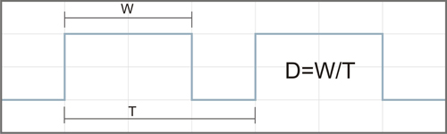
Current only flows through the motor during the "ON" portion of the PWM waveform, so the average voltage applied to the motor is varied by changing the duty cycle. For example, with a 100 V supply and a 30% "ON" time (D=0.3), the average voltage at the motor will be 30 V.
On the following figure you can see the PWM generator circuit for DC motor controller.
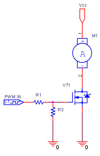
DC motor controller can be implemented using the PWM functionality of DLN-Series USB-IO/I2C/SPI Interface Adapters.
Digital-to-analog converter (DAC)
In electronics, a digital-to-analog converter (DAC or D-to-A) is a device for converting a digital (usually binary) code to an analog signal (current, voltage or electric charge). You can use DAC for testing circuits and amplifiers or for generating the high complexity signals.
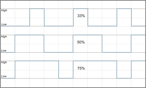
Digital to analog converter can be easily implemented with Pulse Width Modulation (PWM). On the following figure you can see three PWM signals with different duty cycles. The duty cycle describes the proportion of positive pulse width to the period. PWM waveforms with 33%, 50% and 75% of duty cycle are shown below. These three PWM signals can be converted to three different analog values, at 33%, 50%, and 75% of the full strength. For instance, when the voltage level is 5V and the duty cycle is 50%, digital to analog converter outputs 2.5V.
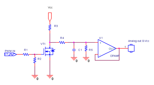
The simplest saving digital to analog converter circuit with high-resistance output is presented on the following schematics:

The next figure shows the digital to analog converter circuit with low-resistance output:

To get the DAC with the voltage range different from 5V, you can use the circuit from the following schematics:
Analog Inputs (ADC Module) Overview
Analog Reference Voltage
GPIO-24 analog to digital converter can measure input voltage levels from VRefLow up to VRefHi.
There are 4 modes to setup VRef source of GPIO-24 analog to digital converter:
- VRefHi is positive supply voltage (VDD), VRefLow is negative supply voltage (VSS);
- VRefHi is the voltage level on the C.6 (VDD), VRefLow is negative supply voltage (VSS);
- VRefHi is positive supply voltage (VDD), VRefLow is the voltage level on the C.5;
- VRefHi is the voltage level on the C.6, VRefLow is the voltage level on the C.5.
Following requirements are reasonable for each mode:
- Reference Voltage Range (VRefHi – VRefLow) >= 3V;
- Reference Voltage High VSS<VRefHi<VDD;
- Reference Voltage Low VSS – 0.3V<VRefLow<VDD – 3.0V;
- Recommended Impedance of Analog Voltage Source – 2.5k.
With external reference voltage you can achieve better accuracy of measurement than with USB-IO adapter supply voltage. USB-IO adapter supply voltage depends on the voltage level of USB port. When using the external reference voltage, keep in mind that any analog input voltage must not exceed VRefHi.
An inexpensive way to generate VRef is by employing a zener diode (mode 1 VRefHi is the voltage level on the C.6, VRefLow is negative supply voltage (VSS)):

Most common zener diodes offer 5% accuracy. Reverse bias current may be as low as 10 μA. However, larger currents (1 mA - 20 mA) are recommended for stability, as well as lower impedance of the VRef source.
Finally, various reference voltage generator chips (typically using on-chip band-gap reference) are available. They are more accurate.
You can measure larger range of voltage levels if you connect the analog input to the output of a voltage divider. It theory, you can measure an indefinitely large DC and AC voltage levels with the help of resistive dividers. But keep in mind that GPIO-24 adapter does not have galvanic isolation from the PC. The improper connection to the source of high voltage (or current) can damage both the USB-IO adapter and the PC. We don’t recommend to measure voltage above 40V with this USB-IO adapter.
Association Between Analog Input Voltage & ADC Digital Code
USB-IO Interface Adapter ADC module allows conversion of an analog input signal to a corresponding 10-bit digital number. The output of the sample and hold is the input into the converter, which generates the result via successive approximation. The analog to digital conversion can be represented mathematically as:
![]()
where: ADC Code - ADC digital output code; VIn - analog input voltage; VRefHi - high reference voltage; VRefLow - low reference voltage.
We get much simpler expression when VRefLow is equal to zero:
![]()
If VRefHi = 5V and VRefLow = 0, analog to digital conversion can be illustrated by the following diagram:

ADC Module SW Interface
GPIO-24 analog to digital converter is easy to setup and use. The PC software can request the analog input value at any time. You can also configure the analog to digital converter to send the analog input values each n millisecond. If you want to be notified only when the input voltage reaches the preset value, simply specify the low and high threshold values.
ADC Module Configuration
Use GPIO_SET_ADC_MODULE_CFG command to configure the ADC module of USB-IO adapter. With this command you can enable/disable the ADC module and select the analog reference voltage.
When you enable the ADC module, all 5 pins (C.1, C.2, C.5, C.6 and B.3) are switched to analog input mode. If you have previously configured these pins to send events (with the GPIO_SET_ADC_CHANNEL_CFG command), they begin to send events immediately. To reset pins configurations, set the byte 4 to 1.
When you disable the ADC module, the same 5 pins are switched to digital input mode.
You can specify the analog reference voltage in byte 3 of the GPIO_SET_ADC_MODULE_CFG command. If you set this byte to 0, ADC module will use the USB-IO adapter supply voltage (VDD and VSS). If you set this byte to 1, ADC module will use the voltage level on the C.6 (VRefHi) and C.5 (VRefLow) pins.
ADC Channels (Analog Input Pins) Configuration
By default, USB-IO adapter doesn’t send events for analog inputs. With GPIO_GET_ADC_VAL command you can get the current analog input values.
Use GPIO_SET_ADC_CHANNEL_CFG command to instruct USB-IO adapter to send events for particular analog input pin. You can specify different event sending conditions for each pin. By sending conditions we mean low and high thresholds.
Low and high threshold values are specified in bytes 4-7. USB-IO adapter sends events when the analog input value is greater than low threshold and less then high threshold.
REPEAT value is specified in byte 3. If the REPEAT value is equal to zero, USB-IO adapter will send single event when the analog input value reaches the specified interval. The next event is sent after the analog input value exits from the specified interval and enters it again.
If the REPEAT value is non-zero, USB-IO adapter sends events repeatedly each REPEAT milliseconds, while the condition is valid. You can set low threshold to 0 and high threshold to 0x3FF, specifying the whole range of possible values. Thus you can monitor the changes at analog input continuously.
ADC Module Applications
Analog to digital conversion has many applications. You can acquire data from wide range of analog sensors and save it at PC for further processing. You can also implement a real time analog data processing in your software. In conjunction with other USB-IO adapter modules you can implement feedback control over your hardware.
Analog to digital conversion is well utilized for external analog signal reading such as current, voltage, temperature, distance, pressure, or even color information.
Below, we list some of the ADC module applications with detailed instructions on how to implement them:
- DC & AC Voltage Measurement;
- DC & AC Current Measurement;
- Resistance Measurement.
Lamp & LED Dimmer
You can adjust the LED (light-emitting diode) or glow lamp brightness with the help of Pulse Width Modulation (PWM). LED dimming is achieved by turning the LED "ON" and "OFF" at high frequency, so fast that the human eye cannot see the strobe effect. The LED current is proportional to the PWM duty cycle. PWM duty cycle is a percentage measurement of the time when the LED is "ON". If the LED is "ON" for 4 ms and "OFF" for 6 ms, the PWM duty cycle is 40%. The longer the "ON" periods are relative to the "OFF" periods, the brighter the LED appears to the observer.
The LED current is proportional to the duty cycle, but its brightness characteristics depend on the current nonliteraly.
On the following figures you can see circuit examples for LED and DC lamp dimming controller:

You can use PWM interface of DLN-series PC-I2C/SPI/GPIO Adapters to control DC lamps and LEDs dimming from a PC. The output current of USB-IO adapter pins can reach 25mA and it is possible to adjust the LED brightness directly (total current of all outputs should not exceed 260mA).
The next figure illustrates the circuit for direct LED dimmer:

I2C Bus
I2C is a two-wired serial bus developed by Philips (now NXP) in the early '80s. Currently, the I2C bus is widely used for interconnection of single-chip microcontrollers, memory chips (EEPROM), analogue-to-digital and digital-to-analog converters, pressure and temperature sensors as well as a variety of other peripheral devices.
I2C bus specification describes four operating speed categories for bidirectional data transfer:
| Standard-mode (Sm) | a bit rate up to 100 kbit/s |
| Fast-mode (Fm) | a bit rate up to 400 kbit/s |
| Fast-mode Plus (Fm+) | a bit rate up to 1 Mbit/s |
| High-speed mode (Hs-mode) | a bit rate up to 3.4 Mbit/s |
I2C bus uses two lines - SDA (data line) and SCL (clock line).

The data is transmitted between two devices - Master and Slave. Master initiates data transfer and generates the synchronization signals. Slave begins data transmission only after master requests it.
Multiple master and slave devices can be connected to the same bus. Later we will discuss the role of each of them, but now it is important to understand how they can transmit data on the same wire, avoiding conflicts.
All devices are connected to the bus via an open collector or open drain. With this connection, the device may output either a logic zero or nothing at all (the output is in the high impedance state).
If outputs of all connected devices are in the high-impedance state, the two external pull-up resistors Rp will hold the lines at high voltage level (logic 1 state). A typical value for these resistors ranges from 1 K to 10 K.

If one or more devices output logic 0, they set the line voltage to low level. The bus is considered to be free when no transmission happens and both lines are in the logic 1 state.
In later chapters, we will examine in detail a variety of options for connecting devices to the I2C bus. Now let's move on and study the I2C protocol by the example of one data byte transmission from the I2C bus master to the slave.

This waveform can be divided into seven parts:
- generation of the START (S) condition
- transmission of the slave device address (0x51)
- data direction bit (read or write)
- acknowledgment (ACK) of the slave device address
- transmission of the data byte
- acknowledgment (ACK) of the data byte
- generation of the STOP (P) condition
We will discuss all seven parts of this waveform in I2C Byte Transfer section. Now lets turn our attention to the transmission of one data bit by the I2C bus.

While transferring data, values on the SDA line are changed when the SCL line is LOW. When the SCL line is HIGH, the receiver reads the data bit (the state of the SDA line). At this point the value of the SDA line must be stable.
I2C Byte Transfer
Let’s examine the waveform of transaction where I2C Master transmits one byte of data to the I2C Slave device.

As we saw in the previous section, the data on the SDA line can be changed when the clock signal on the SCL line is LOW. Exceptions for this rule are START and STOP conditions. There is also a repeated START (Sr) condition, but it will be discussed later.
START condition (S) notifies the Slaves on the transaction beginning. To generate a START condition, the master changes the SDA line from one to zero leaving the SCL line HIGH. After that the Master outputs zero on the SCL line to prepare the bus for transmission of the first bit.

The first seven bits, which follow after START condition, contain I2C slave address. As any other data, the address is transmitted sequentially, starting with the most significant bit (MSB) and ending with the least significant bit (LSB). Each Slave device, which is connected to the I2C bus, must have a unique address. This transaction involves the device with address 1010001 (0x51). All other slaves wait for the STOP condition.

The eighth bit of the first byte defines the direction of transmission. In our case, it is set to zero. This means that the data is transmitted from the Master to the Slave (the write operation). The direction of transmission is set by the Master.

Every eight bits of data (including the address and transmission direction byte) must be followed by the acknowledge bit (ACK). This bit is set by the receiver. In our case, the byte was transferred by the Master, so the Slave sets the acknowledge bit to 0. The Master generates the clock pulse for the acknowledge bit (as well as all the other clocks).

There are three cases when the address byte is not acknowledged (high level on the SDA line):
- The Slave device with this address is not connected to the bus.
- The Slave does not support this transfer direction (write in our case). There are a number of devices that support only read operations. For example, some temperature and pressure sensors.
- The Slave is currently busy with processing of previous command and it is not ready to receive the new one. In some cases the Acknowledge can be delayed by the Slave by holding the SCL line at zero. But we'll discuss this in the synchronization section.
Regardless of the lack of acknowledgment reasons, the Master must generate a STOP condition and free the bus.
After acknowledgment of the address byte, the Master can transmit the first data byte. The data byte must be acknowledged by the Slave as well.
When the transmission is finished, the Master generates a STOP condition and releases the bus. STOP condition is generated by the change of the SDA line from low to high while the SCL line is high. To prepare for the STOP condition, the Master must set the SDA line to zero during the low phase of the clock.

Let’s examine the waveform of transaction where I2C Master transmits one byte of data to the I2C Slave device.
As we saw in the previous section, the data on the SDA line can be changed when the clock signal on the SCL line is LOW. Exceptions for this rule are START and STOP conditions. There is also a repeated START (Sr) condition, but it will be discussed later.
START condition (S) notifies the Slaves on the transaction beginning. To generate a START condition, the master changes the SDA line from one to zero leaving the SCL line HIGH. After that the Master outputs zero on the SCL line to prepare the bus for transmission of the first bit.
The first seven bits, which follow after START condition, contain I2C slave address. As any other data, the address is transmitted sequentially, starting with the most significant bit (MSB) and ending with the least significant bit (LSB). Each Slave device, which is connected to the I2C bus, must have a unique address. This transaction involves the device with address 1010001 (0x51). All other slaves wait for the STOP condition.
The eighth bit of the first byte defines the direction of transmission. In our case, it is set to zero. This means that the data is transmitted from the Master to the Slave (the write operation). The direction of transmission is set by the Master.
Every eight bits of data (including the address and transmission direction byte) must be followed by the acknowledge bit (ACK). This bit is set by the receiver. In our case, the byte was transferred by the Master, so the Slave sets the acknowledge bit to 0. The Master generates the clock pulse for the acknowledge bit (as well as all the other clocks).
There are three cases when the address byte is not acknowledged (high level on the SDA line):
- The Slave device with this address is not connected to the bus.
- The Slave does not support this transfer direction (write in our case). There are a number of devices that support only read operations. For example, some temperature and pressure sensors.
- The Slave is currently busy with processing of previous command and it is not ready to receive the new one. In some cases the Acknowledge can be delayed by the Slave by holding the SCL line at zero. But we'll discuss this in the synchronization section.
Regardless of the lack of acknowledgment reasons, the Master must generate a STOP condition and free the bus.
After acknowledgment of the address byte, the Master can transmit the first data byte. The data byte must be acknowledged by the Slave as well.
When the transmission is finished, the Master generates a STOP condition and releases the bus. STOP condition is generated by the change of the SDA line from low to high while the SCL line is high. To prepare for the STOP condition, the Master must set the SDA line to zero during the low phase of the clock.
I2C Address
Every slave device, connected to the I2C bus, must have an unique I2C address. The I2C address can be either 7-bits or 10-bits long.
You can specify the I2C address in slaveDeviceAddress parameter when you call DlnI2cMasterWrite() or DlnI2cMasterRead() function.
If you use I2C slave interface of a DLN-series adapter, call DlnI2cSlaveSetAddress() to configure the I2C address. You can specify several I2C slave addresses. DLN-series adapter will respond to any of these addresses. After I2C master generates Stop Condition, DLN series adapter sends DLN_I2C_SLAVE_WRITE_EV or DLN_I2C_SLAVE_READ_EV event to your application. These events contain the I2C address in the slaveAddress field.
7-bit I2C Addressing
The first byte (immediately after the START condition) contains the I2C slave address.
The I2C address is 7-bits long. It is transmitted in the seven most significant bits (MSB). The last (eighth bit) of the I2C address byte is a data direction bit - a 'zero' indicates a transmission (I2C WRITE), a 'one' indicates a request for data (I2C READ).

You have to specify the 7-bit I2C slave address when you call the DlnI2cMasterRead() or DlnI2cMasterWrite() function. DLN-series PC-I2C adapters automatically add the direction bit. In fact the provided I2C address is shifted left and is supplemented by 0 (for I2C write transactions) or by 1 (for I2C read transactions).
DLN-series adapters can scan the bus for I2C addresses of the connected slave devices. Call the DlnI2cMasterScanDevices() function to get the list of I2C addresses.
10-bit I2C Addressing
With 7-bit addressing only 112 I2C slave addresses are available. To prevent address clashes Philips Semiconductors (now NXP Semiconductors) has introduced a 10 bit address scheme. Devices with 7-bit and 10-bit addresses can be connected to the same I2C-bus.
The 10-bit address is transmitted within the first two bytes following a START condition or a repeated START condition.

Five most significant bits of the first address byte are predefined (1111 0). I2C slave devices with 7-bit addressing ignore transactions with the first byte in the form of '1111 0XXX'.
The I2C address occupies bits 5 and 6 of the first byte and the eight bits of the second byte.
The transfer direction (read or write) is specified in the eighth bit of the first byte. As in the case of 7-bit I2C address, a 'zero' indicates a transmission (I2C WRITE), a 'one' indicates a request for data (I2C READ).
Slave devices with 10-bit I2C addressing will react to a general call in the same way as slave devices with 7-bit I2C addressing. I2C master devices can transmit the 10-bit I2C address after a general call.
I2C General Call Address
The general call address is used to address all I2C slave devices simultaneously. If I2C slave device doesn't support general call addressing, it ignores this transaction and doesn't issue an acknowledgment. The I2C master devise can't determine how many slave devices acknowledge the general call address.
You can enable the I2C general call address support for I2C slave interface with the DlnI2cSlaveGeneralCallEnable() function.
Reserved I2C slave addresses
There are 16 reserved I2C addresses. These addresses corresponds to one of the two patters: 0000XXX or 1111XXX. The table below describes the purposes of the most commonly used reserved I2C addresses:
| I2C Slave Address | R/W | Bit Description |
|---|---|---|
| 0000 000 | 0 | general call address |
| 0000 000 | 1 | START byte[ |
| 0000 001 | X | CBUS address |
| 0000 010 | X | reserved for different bus format |
| 0000 011 | X | reserved for future purposes |
| 0000 1XX | X | Hs-mode master code |
| 1111 1XX | X | reserved for future purposes |
| 1111 0XX | X | 10-bit slave address |
The full list of I2C address assignments you can see at I2C Address Allocation Table page or i2c-address-allocation-table.pdf document.
I2C Address Allocation Table
The group number represents the hexadecimal equivalent of the four most significant bits of the slave address (A6-A3).
| GROUP(1) | TYPE NUMBER | DESCRIPTION | ||
|---|---|---|---|---|
| Group 0 (0000) | ||||
| 0 | 0 | 0 | - | General call address |
| X | X | X | - | Reserved addresses |
| Group 1 (0001) | ||||
| 1 | A1 | A0 | SAA2530 | ADR/DMX digital receiver |
| 1 | A1 | A0 | TDA8045 | QAM-64 demodulator |
| Group 2 (0010) | ||||
| 0 | 0 | A0 | SAA4700/T | VPS dataline processor |
| 0 | 0 | A0 | SAA5233 | Dual standard PDC decoder |
| 0 | 0 | 1 | SAA5243 | Computer controlled teletext circuit |
| 0 | 0 | 1 | SAA5244 | Integrated VIP and teletext |
| 0 | 0 | 1 | SAA5245 | 525-line teletext decoder/controller |
| 0 | 0 | 1 | SAA5246A | Integrated VIP and teletext |
| 0 | 0 | 1 | SAA5249 | VIP and teletext controller |
| 0 | A1 | A0 | CCR921 | RDS/RBDS decoder |
| 0 | A1 | A0 | SAF1135 | Dataline 16 decoder for VPS (call array) |
| 1 | 0 | 0 | SAA5252 | Line 21 decoder |
| 1 | 1 | A0 | SAB9075H | PIP controller for NTSC |
| Group 3 (0011) | ||||
| 0 | 0 | A0 | SAA7370 | CD-decoder plus digital servo processor |
| 0 | A1 | A0 | PCD5096 | Universal codec |
| 0 | 1 | A0 | SAA2510 | Video-CD MPEG-audio/video decoder |
| 0 | 1 | 1 | PDIUSB11 | Universal serial bus |
| 1 | 0 | 1 | SAA2502 | MPEG audio source decoder |
| 1 | 1 | A0 | SAA1770 | D2MAC decoder for satellite and cable TV |
| Group 4 (0100) | ||||
| 0 | 0 | 0 | SAA6750 | MPEG2 encoder for Desk Top Video (=SAA7137) |
| 0 | 0 | 0 | TDA9177 | YUV transient improvement processor |
| 0 | 0 | 0 | TDA9178 | YUV transient improvement processor |
| 0 | 0 | A0 | PCA1070 | Programmable speech transmission IC |
| 0 | A1 | A0 | PCF8575 | Remote 16-bit I/O expander |
| 0 | A1 | A0 | PCF8575C | Remote 16-bit I/O expander |
| 0 | A1 | A0 | SAA1300 | Tuner switch circuit |
| A2 | A1 | A0 | TDA8444 | Octuple 6-bit DAC |
| A2 | A1 | A0 | PCF8574 | 8-bit remote I/O port (I2C-bus to parallel converter) |
| 1 | 0 | A0 | PCD3311C | DTMF/modem/musical tone generator |
| 1 | 0 | A0 | PCD3312C | DTMF/modem/musical tone generator |
| 1 | 1 | 1 | PCD5002 | Pager decoder |
| Group 6 (0110) | ||||
| 0 | 0 | 0 | SAA5301 | MOJI processor for Japan/China |
| 0 | 1 | 1 | PCE84C467/8 | 8-bit CMOS auto-sync monitor controller |
| 0 | 1 | 1 | PCE84C882 | 8-bit microcontroller for monitor applications |
| 0 | 1 | 1 | PCE84C886 | 8-bit microcontroller for monitor applications |
| Group 7 (0111) | ||||
| 0 | 0 | A0 | SAA7140B | High performance video scaler |
| 0 | 0 | A0 | PCF8533 | Universal LCD driver for low multiplex rates |
| 0 | 0 | A0 | PCF8576 | 16-segment LCD driver 1:1 - 1:4 Mux rates |
| 0 | 0 | A0 | PCF8576C | 16-segment LCD driver 1:1 - 1:4 Mux rates |
| 0 | A1 | A0 | SAA1064 | 4-digit LED driver |
| A2 | A1 | A0 | PCF8574A | 8-bit remote I/O port (I2C-bus to parallel converter) |
| 0 | 1 | 0 | PCF8577C | 32/64-segment LCD display driver |
| 0 | 1 | A0 | PCF2103 | LCD controller/driver |
| 0 | 1 | A0 | PCF2104 | LCD controller/driver |
| 0 | 1 | A0 | PCF2105 | LCD controller/driver |
| 0 | 1 | A0 | PCF2113 | LCD controller/driver |
| 0 | 1 | A0 | PCF2119 | LCD controller/driver |
| 0 | 1 | A0 | SAA2116 | LCD controller/driver |
| 1 | 0 | A0 | PCF8531 | 34 X 128 pixel matrix driver |
| 1 | 0 | A0 | PCF8548 | 65 X 102 pixels matrix LCD driver |
| 1 | 0 | A0 | PCF8549 | 65 X 102 pixels matrix LCD driver |
| 1 | 0 | A0 | PCF8578/9 | Row/column LCD dot matrix driver/display |
| 1 | 0 | A0 | PCF8568 | LCD row driver for dot matrix displays |
| 1 | 0 | A0 | PCF8569 | LCD column driver for dot matrix displays |
| 1 | A1 | A0 | PCF8535 | 65 X 133 pixel matrix LCD driver |
| 1 | 1 | A0 | OM4085 | Universal LCD driver for low multiplex rates |
| 1 | 1 | A0 | PCF8566 | 96-segment LCD driver 1:1 - 1:4 Mux rates |
| Group 8 (1000) | ||||
| 0 | 0 | 0 | TEA6300 | Sound fader control and preamplifier/source selector |
| 0 | 0 | 0 | TEA6320/1/2/3 | Sound fader control circuit |
| 0 | 0 | 0 | TEA6330 | Tone/volume controller |
| 0 | 0 | A0 | NE5751 | Audio processor for RF communication |
| 0 | 0 | A0 | TDA8421 | Audio processor |
| 0 | 0 | A0 | TDA9860 | Hi-fi audio processor |
| 0 | 0 | 1 | TDA8424/5/6 | Audio processor |
| 0 | 1 | 0 | TDA8415 | TV/VCR stereo/dual sound processor |
| 0 | 1 | 0 | TDA8417 | TV/VCR stereo/dual sound processor |
| 0 | 1 | 0 | TDA9840 | TV stereo/dual sound processor |
| 0 | 1 | A0 | TDA8480T | RGB gamma-correction processor |
| 1 | 0 | 0 | TDA4670/1/2 | Picture signal improvement (PSI) circuit |
| 1 | 0 | 0 | TDA4680/5/7/8 | Video processor |
| 1 | 0 | 0 | TDA4780 | Video control with gamma control |
| 1 | 0 | 0 | TDA4885 | 150 MHz video controller |
| 1 | 0 | 0 | TDA8442 | Interface for colour decoder |
| 1 | 0 | 1 | TDA8366 | Multistandard one-chip video processor |
| 1 | 0 | 1 | TDA8373 | NTSC one-chip video processor |
| 1 | 0 | 1 | TDA8374 | Multistandard one-chip video processor |
| 1 | 0 | 1 | TDA8375/A | Multistandard one-chip video processor |
| 1 | 0 | 1 | TDA8376/A | Multistandard one-chip video processor |
| 1 | 0 | 1 | TDA9161A | Bus-controlled decoder/sync. processor |
| 1 | A1 | 1 | SAA7151B | 8-bit digital multistandard TV decoder |
| 1 | A1 | 1 | SAA7191B | Digital multistandard TV decoder |
| 1 | A1 | 1 | SAA9056 | Digital SCAM colour decoder |
| 1 | A1 | 1 | TDA9141/3/4 | Alignment-free multistandard decoder |
| 1 | A1 | 1 | TDA9160 | Multistandard decoder/sync. processor |
| 1 | A1 | 1 | TDA9162 | Multistandard decoder/sync. processor |
| 1 | 1 | 0 | TDA4853/4 | Autosync deflection processor |
| 1 | 1 | 0 | TDA9150B | Deflection processor |
| 1 | 1 | 0 | TDA9151B | Programmable deflection processor |
| 1 | 1 | A0 | TEA6360 | 5-band equalizer |
| 1 | 1 | A0 | TDA8433 | TV deflection processor |
| Group 9 (1001) | ||||
| A2 | A1 | A0 | PCF8591 | 4-channel, 8-bit Mux ADC and one DAC |
| A2 | A1 | A0 | TDA8440 | Video/audio switch |
| A2 | A1 | A0 | TDA8540 | 4 X 4 video switch matrix |
| 1 | A1 | A0 | TDA8752 | Triple fast ADC for LCD |
| 1 | 1 | A0 | SAA7110A | Digital multistandard decoder |
| Group A (1010) | ||||
| 0 | 0 | A0 | SAA7199B | Digital multistandard encoder |
| 0 | 1 | 0 | TDA8416 | TV/VCR stereo/dual sound processor |
| 0 | 1 | A0 | TDA9850 | BTSC stereo/SAP decoder |
| 0 | 1 | A0 | TDA9855 | BTSC stereo/SAP decoder |
| 0 | 1 | 1 | TDA9852 | BTSC stereo/SAP decoder |
| 1 | 0 | 0 | TDA9610 | Audio FM processor for VHS |
| 1 | 0 | 0 | TDA9614H | Audio processor for VHS |
| 1 | A1 | 0 | SAA7186 | Digital video scaler |
| 1 | 0 | 1 | PCA8516 | Stand-alone OSD IC |
| 1 | 1 | 1 | SAA7165 | Video enhancement D/A processor |
| 1 | 1 | 1 | SAA9065 | Video enhancement and D/A processor |
| Group B (1011) | ||||
| 0 | 0 | A0 | SAA7199B | Digital multistandard encoder |
| 0 | 1 | 0 | TDA8416 | TV/VCR stereo/dual sound processor |
| 0 | 1 | A0 | TDA9850 | BTSC stereo/SAP decoder |
| 0 | 1 | A0 | TDA9855 | BTSC stereo/SAP decoder |
| 0 | 1 | 1 | TDA9852 | BTSC stereo/SAP decoder |
| 1 | 0 | 0 | TDA9610 | Audio FM processor for VHS |
| 1 | 0 | 0 | TDA9614H | Audio processor for VHS |
| 1 | A1 | 0 | SAA7186 | Digital video scaler |
| 1 | 0 | 1 | PCA8516 | Stand-alone OSD IC |
| 1 | 1 | 1 | SAA7165 | Video enhancement D/A processor |
| 1 | 1 | 1 | SAA9065 | Video enhancement and D/A processor |
| Group C (1100) | ||||
| 0 | 0 | 1 | TEA6100 | FM/IF for computer-controlled radio |
| 0 | 1 | 0 | TEA6821/2 | Car radio AM |
| 0 | 1 | 0 | TEA6824T | Car radio IF IC |
| 0 | A1 | A0 | TSA5511/2/4 | 1.3 GHz PLL frequency synthesizer for TV |
| 0 | A1 | A0 | TSA5522/3M | 1.4 GHz PLL frequency synthesizer for TV |
| 0 | 1 | A0 | TDA8735 | 150 MHz PLL frequency synthesizer |
| 0 | 1 | A0 | TSA6057 | Radio tuning PLL frequency synthesizer |
| 0 | 1 | A0 | TSA6060 | Radio tuning PLL frequency synthesizer |
| 0 | 1 | A0 | UMA1014 | Frequency synthesizer for mobile telephones |
| 1 | 0 | 0 | TDA8722 | Negative video modulator with FM sound |
| Group D (1101) | ||||
| 0 | 0 | A0 | TDA8043 | QPSK demodulator and decoder |
| 0 | 0 | A0 | TDA9170 | YUV processor with picture improvement |
| 0 | A1 | A0 | PCF8573 | Clock/calendar |
| A2 | A1 | A0 | TDA8443A | YUV/RGB matrix switch |
| 0 | 1 | A0 | TDA8745 | Satellite sound decoder |
| 1 | 0 | 0 | TDA1551Q | 2 ´ 22 W BTL audio power amplifier |
| 1 | A1 | A0 | TDA4845 | Vector processor for TV-pictures tubes |
| 1 | A1 | A0 | UMA1000T | Data processor for mobile telephones |
| 1 | 1 | A0 | PCD4440 | Voice scrambler/descrambler for mobile telephones |
| Group E (1110) | ||||
| 0 | 0 | 0 | PCD3316 | Caller-ID on Call Waiting (CIDCW) receiver |
| 0 | 0 | 0 | TDA9177 | 2nd address for LTI (1st is '40') |
| 0 | 0 | 0 | TDA9178 | 2nd address for LTI (1st is '40') |
| 0 | 0 | A0 | SAA7192 | Digital colour space-converter |
| Group F (1111) | ||||
| X | X | X | - | Reserved addresses |
| Group 0 to F (0000 to 1111) | ||||
| X | X | X | PCF8584 | I2C-bus controller |
Note
1. X = Don't care, A = Programmable address bit, P = Page selection bit
I2C Bus Specification
The most recent I2C bus specification (revision 4) was released at February 2012. In this I2C specification NXP Semiconductors introduced the unidirectional I2C bus and Ultra Fast-mode (UFm), with I2C bit rate up to 5 Mbit/s.
Download I2C Specification (version 4.0)
Ultra Fast-mode devices use push-pull drivers (the bidirectional bus requires open-drain output buffers) and eliminates the pull-up resistors. Ultra Fast-mode I2C devices are not compatible with I2C specification for bidirectional bus.
I2C Bus Specification History
The original I2C bus specification was released in 1982 by Philips Semiconductors. Its main purpose was to provide an easy way to connect a CPU to peripheral chips in a TV-set. Philips Semiconductors was one of the main manufacturers of consumer electronics in the early 1980's. This version of I2C specification covered Standard mode and Low-speed mode. The low speed mode has been omitted in the version 1.0 of I2C specification.
At 1992 Philips Semiconductor released the I2C Bus Specification Version 1.0. In this version of I2C specification Philips Semiconductor removed the low-speed mode and added the Fast-mode (bit rate up to 400 kbis/s). In addition to 7-bit addressing, 10-bit addressing was introduced (to allow additional 1024 slave addresses).
At April 1995 Philips Semiconductor published the application note "The I2C-bus and how to use it (including I2C specifications)"
At December 1998 Philips Semiconductor released The I2C Bus Specification Version 2.0. The major changes in this version include addition of High-speed mode (I2C transfer rate up to 3.4 Mbit/s) and usage of bus voltage related levels instead of fixed input levels.
At August 1999 Philips Semiconductors published the list of assigned I2C addresses.
At January 1990 Philips Semiconductors reviewed some timing parameters for High-speed mode and released The I2C Bus Specification Version 2.1. The clock stretching after the START condition was also enabled in this I2C specification release.
At January 2003, at DesignCon 2003 in San Jose, Philips Semiconductor presented the I2C Manual. This I2C manual contains overview of different serial buses, their pros and cons and practical hints for I2C bus implementation and usage.
- Download I2C Bus Manual
- Download I2C Bus Overview Slide from DesignCon 2003 TecForum
At 1st September 2006, Philips Semiconductors CEO Frans van Houten revealed that the company will move forward as NXP Semiconductors. From this date all updates to I2C specification were published under the new company name.
At June 2007 NXP Semiconductors released the version 3 of I2C specification. In this version, they introduced the Fast-mode Plus (Fm+) specification. The Fast-mode Plus supports I2C transfers with the rate up to 1 Mbit/s. NXP Semiconductors also moved level shifting information to a separate application note.
- Download I2C Bus Specification (version 3.0)
- Download application note "Level shifting techniques in I2C bus design"
Finally, at February 2013, NXP Semiconductors released The I2C Bus Specification Version 4. In this version was added the unidirectional bus and Ultra Fast-mode (UFm), with a bit rate up to 5 MBit/s. This is the latest version of the I2C bus specification.
USB-I2C Adapters that conform to I2C Bus Specification
All DLN-series PC-I2C adapters conform to I2C Bus Specification (ver. 4) Fast-mode transfer rate.
DLN-1 and DLN-2 USB-I2C adapters also conform to Fast-mode Plus specification (I2C interface speed up to 1 Mbit/s).
We have tested DLN-4M and DLN-4S adapters at frequencies up to 1 MHz and have proved to work well, but their I2C lines have 6 mA current limitations. This limitation can affect I2C bus communication at Fast-mode Plus speed if long wires are used or many slave devices are connected to the same USB-I2C adapter.
I2C Bus Speed
In the beginning the I2C bus was limited to the speed of 100 kbps. Now this I2C speed limitation is called the Standard-mode (Sm)
To keep up with the ever-increasing performance requirements of new ICs, Philip Semiconductors (now NXP Semiconductors) have reviewed the I2C frequency limitations. In 1992 the I2C bus speed was increased to 400 kbps, introducing the term Fast-mode (Fm).
Lately the I2C bus frequency has been increased several more times. At nowadays I2C specification defines the following I2C speeds for bidirectional bus:
| Standard-mode (Sm) | I2C speed up to 100 kbit/s |
| Fast-mode (Fm) | I2C speed up to 400 kbit/s |
| Fast-mode (Fm) | I2C speed up to 1 Mbit/s |
| High-speed mode (Hs-mode) | I2C speed up to 3.4 Mbit/s |
At February 2012 NXP Semiconductors(formerly Philips Semiconductors) released the revision 4 of I2C bus specification. In this revision NXP Semiconductors has introduced the unidirectional bus with Ultra Fast-mode (I2C speed up to 5 Mbit/s)
I2C Speed is NOT Just Frequency
Most vendors in their manuals specify maximum I2C bus frequency. By I2C frequency they mean the frequency on the SCL line during a single byte transmission. They don't mention the delays between successive bytes transmission. Sometimes the delays between bytes can be longer than the byte itself.
I2C Bus Interface
 The I2C bus was developed by Philips Semiconductors (now NXP Semiconductors) as a simple serial bidirectional, 8-bit oriented, 2-wire bus.
Each device is recognized by a unique address and can operate as either a receiver-only device (e.g., an LCD driver) or a transmitter with the capability to both receive and send information (such as memory). Transmitters and/or receivers can operate in either master or slave mode, depending on whether the chip has to initiate a data transfer or is only addressed. The I2C is a multi-master bus and can be controlled by more than one bus master connected to it.
Depending on the speed mode the I2C bus can operate at the following frequencies:
| I2C Bus Standard Mode | Transfer rate up to 100 kbit/s. |
| I2C Bus Fast Mode | Transfer rate up to 400 kbit/s. |
| I2C Bus Fast Mode Plus (Fm+) | Transfer rate up to 1 Mbit/s. |
| I2C Bus High Speed Mode | Transfer rate up to 3.4 Mbit/s. |
All DLN-series I2C bus adapters support transfer rate up to 1 Mbit/s (Fast-mode Plus).
The I2C bus requires two bus lines:
| SDA | a serial data line |
| SCL | a serial clock line |
I2C Bus Derivative Technologies
Due to the great success and applicability of the I2C bus, Atmel and other vendors implement the same protocol on various system-on-chip processors under the different names: TWI (Two Wire Interface) or TWSI (Two-Wire Serial Interface).
The I2C bus is used in a variety of control architectures such as:
- System Management Bus (SMBus)
- Power Management Bus (PMBus)
- Intelligent Platform Management Interface (IPMI)
- Advanced Telecom Computing Architecture (ATCA)
These I2C bus implementations have differences in voltage and clock frequency ranges, and may have interrupt lines.
SPI Bus
The Serial Peripheral Interface (SPI) is a synchronous serial data interface, developed by Motorola. It is used for connecting various peripheral devices. SPI operates either in full-duplex or in half-duplex mode and can transfer data over short distances at high speeds. During data transfer devices can work either in master or in slave mode. The source of synchronization is the system clock, which is generated by the master. The SPI interface allows to connect one or more slave devices to a single master device via the same bus.

SPI Key Features
- Read, write and full-duplex (simultaneous read/write) data transactions;
- SPI master and SPI slave configuration;
- Configurable SPI bus clock polarity, phase and frequency;
- Configurable number of bits to transfer;
- Communication with serial external devices (ADC and DAC, RTC, temperature and pressure sensors, LCD controller, etc.).
SPI Benefits
- SPI is considered the fastest synchronous serial data transfer interface;
- SPI is a very simple communication protocol;
- Supports full-duplex communication;
SPI Drawbacks
- Requires more traces on the board (X + 3, where X is the number of slave devices);
- No hardware flow control;
- No slave acknowledgment;
- May prone to noise spikes causing faulty communication.
SPI Structure
To understand the SPI interface structure, first, we need to look at its lines. There are 4 lines in total (2 data lines and 2 service lines):

- CS (chip select) or SS (slave select) line - allows/disallows operation with slave device.
- MISO (Master input slave output) data line - data can be transferred from slave to master over this line.
- MOSI (Master output slave input) data line - data can be transferred from master to slave device over this line.
- CLK (clock) line - Clock signal.
When the signal from CS service line is inverted (equals to 1) slave device is inactive, when CS signal equals to 0, master device can transfer or receive data to/from slave device. This line allows to connect several slave devices to master, so we can choose the slave device for data transfer over SPI interface.
Another service line is CLK. It generates clock signal. While data is transferred over SPI interface, CLK line is also generating clock signal. Its frequency determines the data transfer speed over SPI. CLK signal is transferred with the same frequency as data flows. Thus there is no need to synchronize the transfer speed of master and slave devices.
MOSI (Master Output Slave Input) line - data line which is used for data transferring from master device to slave device.
MISO (Master Input Slave Output) line - data line, which is used for data transferring from slave device to master device.
Configurable SPI Delays
Sometimes slave devices need additional time to process data. In order to provide this time DLN-series adapters can insert delays at different data transmission stages. Those are delay between frames, delay after slave selection and delay between slave selection. All of the delays are set in nanoseconds and have to be adjusted only once. After configuring the delays are applied to all the SS lines.
Delay Between SPI Frames

In case a slave device is not fast enough to process continuously incoming data, a user can configure the DLN adapter to insert delays between each two consecutive frames. This gives the slave device additional time to process the data from the previous frame. Once enabled, the delay is inserted after each frame. The delay value is adjusted using the DlnSpiMasterSetDelayBetweenFrames() function. The current delay between frames value can be retrieved by calling the DlnSpiMasterGetDelayBetweenFrames() function.
Delay After Slave Selection

When SPI slave device needs additional time for initialization, a Delay After Slave Selection (SS) can be used. When enabled, it is placed after an SS line assertion and before the first frame transmission. The delay value is adjusted using the DlnSpiMasterSetDelayAfterSS() function. You can retrieve the current delay value by calling the DlnSpiMasterGetDelayAfterSS() function.
Delay Between Slave Selection

Delay Between Slave Selection is inserted between one SS line release and assertion of another SS line. The delay value is adjusted using the DlnSpiMasterSetDelayBetweenSS() function, and can be retrieved using the DlnSpiMasterGetDelayBetweenSS() function.
SPI Frames
A frame is a single portion of data sent through SPI bus. Some of the DLN adapters support adjustable frame size. The frame data are transferred starting from the most significant bit and up to the least significant bit.

In case the frame size is set to 8 bits or less, only one byte is needed to store the frame data. If the frame size is lesser than 8 bits, the least significant bits of the byte will be transferred, while extra (most significant) bits will be discarded, regardless of their content. The DlnSpiMasterReadWrite() function can be called to transmit array of 8-bit and smaller frames.
In case a frame size is 9-16 bits, two bytes are needed to store the frame data. You can allocate an array of up to 128 16-bit integers. These integers must be stored inside the array in Little Endian format. This shouldn't cause a problem, since Little Endian format is used for data storage by most of modern computers. If the frame size is less than 16 bits, 2-byte integers will be used. The least significant bits of the integer will be transferred, while extra (most significant) bits will be discarded, regardless of their content.
The size of the frame does not limit the size of the buffer to be transferred. DlnSpiMasterReadWrite() (DlnSpiMasterReadWrite16()) function accepts buffer sizes of up to 256 bytes. You can call the function several times to send a larger buffer.
Splitting the data transfer into frames allows to set delays and configure SS line release between the frames. By default no delays are set and SS line remains asserted all the time.
SPI Operation Modes
SPI Full Duplex Mode
In full duplex mode SPI master device simultaneously transmits data to a slave and receives data from a slave. This way only a single slave device can be engaged at one time. An SS line is used to select the particular SPI slave device.
 SPI in full duplex mode
SPI in full duplex mode
SPI Half Duplex Mode (Single Read)
In half duplex single read mode SPI master device only receives data from a slave. This way only a single slave device can be engaged at one time. An SS line is used to select the slave device.
 SPI in half duplex single read mode
SPI Half Duplex Mode (Single Write)
In half duplex single write mode SPI master device only transmits data to a slave, and doesn't receive any data from the slave. This way simultaneous operation with several slave devices is possible.
 SPI in half duplex single write mode
SPI Slave Selection
There is different number of available SS lines for each DLN-series adapter. There is 1 SS line for DLN-1 adapter, there are 5 SS lines for DLN-2 and 4 SS lines for DLN-4M/S adapters. If you need more SS lines you can use unengaged GPIO pins as well.
An SS line is used to select an SPI slave device. Slave device is selected by calling the DlnSpiMasterSetSS() function.
Selecting Single SPI Slave Device
If you use the DLN-series adapter in Full Duplex or Half Duplex (Single Read) mode, you can only select one slave device at a time.
In order to deactivate all devices send a 0xFF (1111 1111) value. A slave device can be selected by changing the corresponding bit value to 0.
Example: Slave device #01 can be selected by calling the DlnSpiMasterSetSS() function and passing 0xFD (1111 1101) value as the ss parameter.
Selecting Several SPI Slave Devices At Once
If you use the DLN-series adapter in Half Duplex (Single Write) mode, you can activate several slave devices at once.
A user can address the required slave devices by changing the respective bit values to 0.
Example: Slave device #00 and #02 can be activated by calling the DlnSpiMasterSetSS() function and passing the 0xFA (1111 1010) value as the ss parameter.
Addressing up to 15 SPI Slave Devices
If you connect the ss lines to an external decoder/demultiplexer, you will be able to connect more slave devices to single DLN-series adapter.

In order to use this feature you need an external decoder/demultiplexer (e.g. 74HC4515). With a decoder/demultiplexer connected, the SS lines are used to send a 4-bit value. A user can address the necessary slave by sending its number (values from 0 to 15). The numbers 0 to 14 represent the number of the slave device, while 15 means that no device is selected. This means you can connect up to 15 slave devices to the DLN-series adapter.
Example: Slave device #11, can be activated by calling the DlnSpiMasterSetSS() function and passing the 0xFB (1111 1011) value as the ss parameter.
SPI Transfer Modes
SPI interface allows to transmit and receive data simultaneously on two lines (MOSI and MISO). Clock polarity (CPOL) and clock phase (CPHA) are the main parameters that define a clock format to be used by the SPI bus. Depending on CPOL parameter, SPI clock may be inverted or non-inverted. CPHA parameter is used to shift the sampling phase. If CPHA=0 the data are sampled on the leading (first) clock edge. If CPHA=1 the data are sampled on the trailing (second) clock edge, regardless of whether that clock edge is rising or falling.
CPOL=0, CPHA=0

The data must be available before the first clock signal rising. The clock idle state is zero. The data on MISO and MOSI lines must be stable while the clock is high and can be changed when the clock is low. The data is captured on the clock's low-to-high transition and propagated on high-to-low clock transition.
CPOL=0, CPHA=1

The first clock signal rising can be used to prepare the data. The clock idle state is zero. The data on MISO and MOSI lines must be stable while the clock is low and can be changed when the clock is high. The data is captured on the clock's high-to-low transition and propagated on low-to-high clock transition.
CPOL=1, CPHA=0

The data must be available before the first clock signal falling. The clock idle state is one. The data on MISO and MOSI lines must be stable while the clock is low and can be changed when the clock is high. The data is captured on the clock's high-to-low transition and propagated on low-to-high clock transition.
CPOL=1, CPHA=1

The first clock signal falling can be used to prepare the data. The clock idle state is one. The data on MISO and MOSI lines must be stable while the clock is high and can be changed when the clock is low. The data is captured on the clock's low-to-high transition and propagated on high-to-low clock transition.
SS Line Release Between Frames Theory
By default, SPI data transmission between a master and a slave looks like this.
However, some slave devices require SS line to be released and deasserted between data frames.
In this case an SS line is released after each frame and asserted before the next frame. If delay between frames is specified, the SS line will be released for the whole delay duration. Yet, the line will still be released and asserted between data frames even if this delay is zero.